File Download
Modern semiconductor fabs rely on wafer-level testing to catch defective chips before expensive packaging.
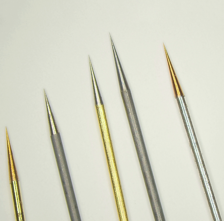
The core contact elements in these tests are custom tungsten probes – often called tungsten needles.
Pure tungsten is ideal for needle probes because of its extreme stiffness, hardness, and durability.
For example, Metal Cutting Corporation notes that tungsten wire has remarkable stiffness even at tiny diameters, giving it the straightness needed for micron-scale probing.
This stiffness means a tungsten needle holds its shape under load, so the tip stays on target over thousands of contacts.
Tektronix also confirms tungsten’s strength and spring-like behavior, stating that tungsten is most commonly used for wafer probing on aluminum pads due to its high hardness and stable contact performance.
In practice, wafer probe testing happens after wafer fabrication but before singulation and packaging.
Each die on the wafer must be tested, and using probes at the wafer stage prevents wasting resources on a bad chip later. As industry experts explain, probing on the wafer is done before the circuits are diced and packaged — and before the costs of those steps are incurred.
Tungsten needles make these tests possible: their ultra-fine tips (<1 μm) can land on bond pads only a few microns wide, and their toughness lets them repeatedly penetrate oxide layers for reliable contact.
Why Tungsten Needles Are Essential in Wafer Testing
- Stiffness for Accuracy: Tungsten’s high elastic modulus means probes stay straight and positioned.
- No Spring-Back: Tungsten wires keep their bent shape under stress, guaranteeing accurate landings.
- Tiny Diameters: Tungsten maintains properties at very small diameters (even <5 μm), enabling ultra-fine tips.
- Hardness & Lifespan: Tungsten’s hardness ensures long probe life and fewer replacements.
- Oxide Penetration: Tungsten tips scrub away oxide to reach the pad metal, ensuring reliable connections.
Custom Probe Designs: Sizes and Tip Shapes
Our custom tungsten needles start at extremely fine dimensions. We can draw 5 μm diameter pure tungsten wire with tip radii as small as 1 μm (±0.5 μm tolerance). Standard probe lengths include 27 mm, 35 mm, and 38 mm. Every parameter – diameter, tip radius, length – can be customized to fit your prober setup.
We also fabricate specialized tip geometries and shank shapes on demand, such as 90°-bend tungsten probes for edge pads, flat tips for broad contacts, hooks for special probing needs, and threaded tungsten stems that mount securely in probe cards. In short, any tungsten shape can be produced – round, plate, hook, or thread – according to customer requirements.
Technical Highlights:
- Tip Diameter: down to 1 μm with ±0.5 μm accuracy
- Lengths: 27, 35, 38 mm standard; custom available
- Geometries: bent, hooked, flat, or threaded
- Material: 99.99% pure tungsten wire (W or W-Re alloy)
Integration into Wafer Test Systems
In wafer test systems, tungsten needles are mounted on a probe card that connects the tester to the wafer. The probe needles carry the signals and are the heart of the assembly. Because of their central role, custom probes often represent the largest portion of probe-card cost. Our tungsten needles provide the exact dimensions and geometry to ensure proper contact force, alignment, and reliability in any fixture, from legacy systems to advanced automated probers.
About Shenzhen Xinxin Precision Equipment Co., Ltd.
At Shenzhen Xinxin Precision Equipment Co., Ltd., we specialize in precision tungsten components for semiconductor testing:
- Custom tungsten parts: needles, shafts, hooks, plates, and threaded rods
- Precision tolerances: tip accuracy within ±0.5 μm
- Flexible production: prototypes or large-scale orders
We work closely with semiconductor manufacturers and procurement engineers to ensure every probe meets stringent standards. Our tungsten needles support wafer testing for ICs, LEDs, and advanced devices.
Contact Us
For inquiries or a custom quote, please contact us via email at info@machinedesign.top or visit our website: machinedesign.top.


